
ack from our Hot Chips 2025 ice cream break, NVIDIA is starting off the second session of machine learning presentations. As with yesterday’s graphics presentation, NVIDIA isn’t so much showing off future hardware as much as they are offering a better lay of the land on their latest generation of hardware that is already on the market. And this afternoon’s session is focused on the GB10 SoC.
NVIDIA Outlines GB10 SoC Architecture at Hot Chips 2025
Powering NVIDIA’s DGX Spark small form factor workstation (née DIGITS), GB10 is a multi-die single-chip solution for high-performance Arm-based workstations. With a GPU die based on the Blackwell architecture and a CPU die built by MediaTek that contains 20 Arm CPU cores. And with both dies built on TSMC’s 3nm process, GB10 is technically the most advanced Blackwell product yet.
NVIDIA is still a GPU company first and foremost. And to that end, Blackwell is the heart and soul of GB10.
In this case, Blackwell has been scaled down to a particularly small configuration. But it still supports all of Blackwell’s marquee features, most notably FP4 support.
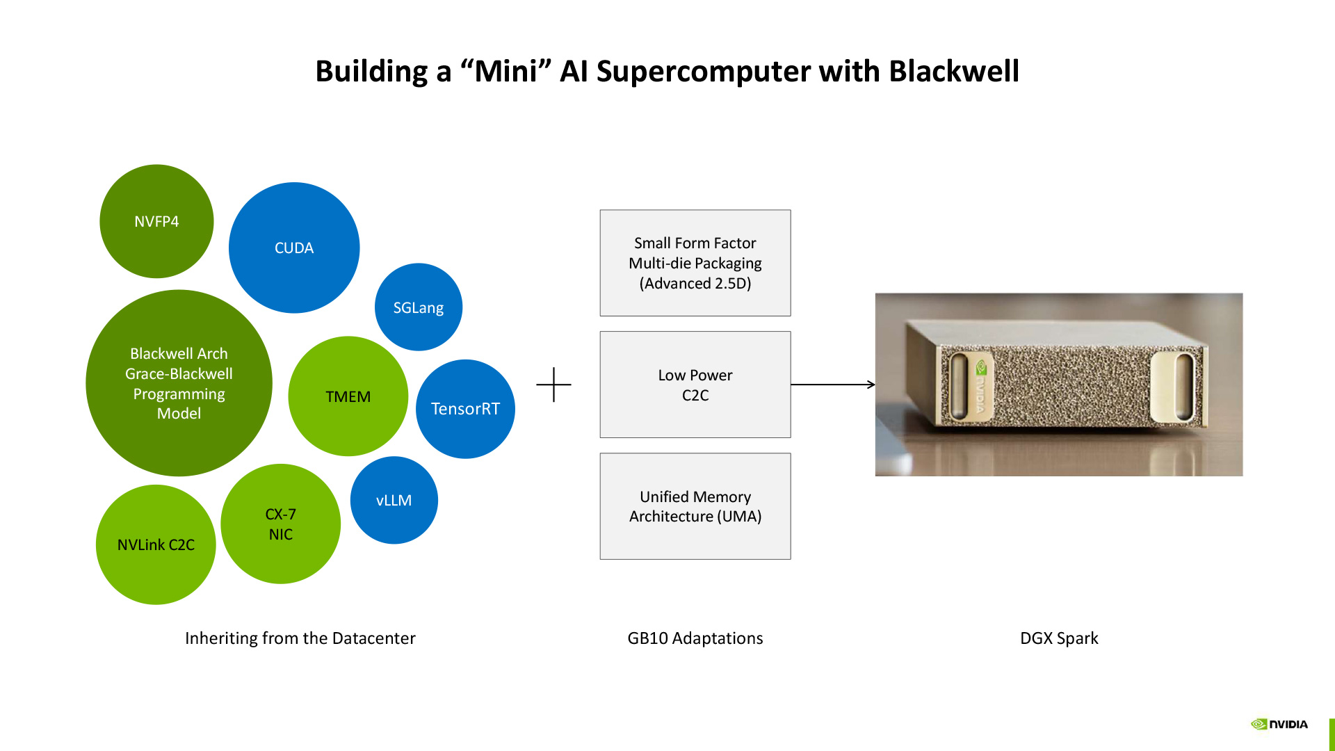
GB10 adds its own technologies to the mix. This includes low-power C2C links and support for a unified memory architecture – one physical and logical memory. And both CPU and GPU dies needed to be placed on a single 2.5D interposer.
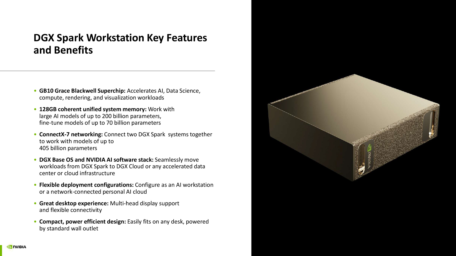
Key benefits and features: 128GB of unified LPDDR5X system memory. Which is enough space for fine-tuning models with up to 70B paramenters.
There’s also a ConnectX-7 NIC to allow two DGX Spark systems to be paired up together to work on even larger models.
And NVIDIA isn’t hiding that DGX Spark is a gateway device – develop and test on a Spark box, and then deploy finished models to DGX Cloud.
It can run off of a standard wall outlet. Compared to server boxes, this is legitimately a notable feature.
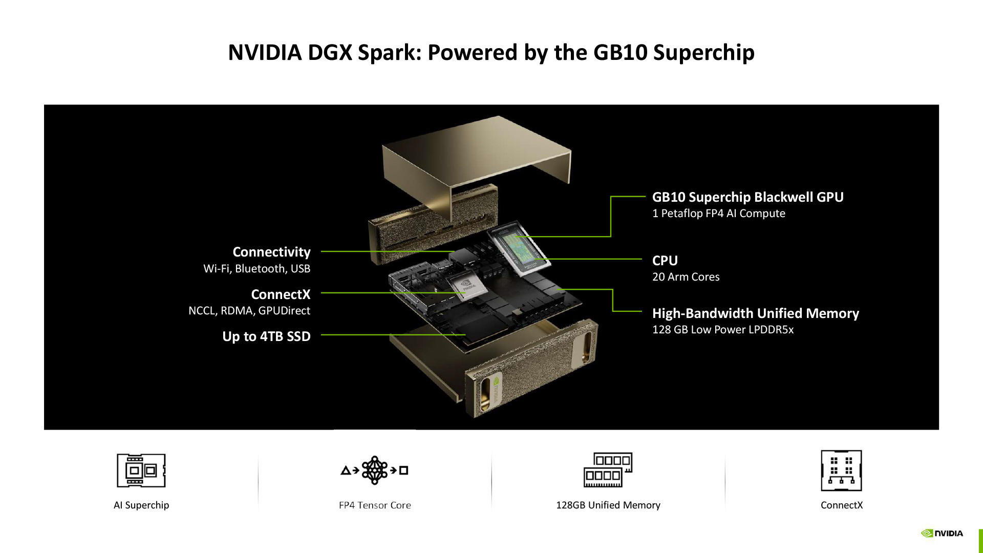
Detailing various specs. 20 CPU cores, up to 4TB SSDs, HBM memory.
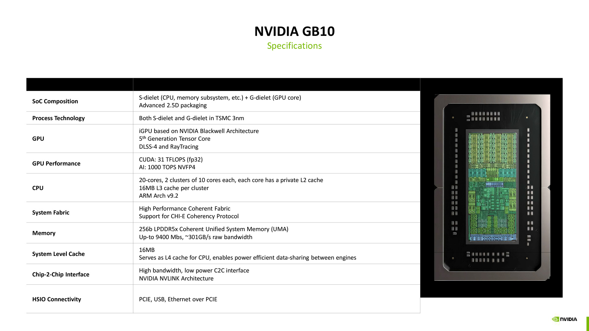
More on specs. Two dies, both built on TSMC 3nm. The GPU supports all of the latest Blackwell features, including DLSS and raytracing. 31 TFLOPS of FP32 performance, or 1000 TFOPS FP4.
The cores are based on Arm’s v9.2 architecture. Though NVIDIA isn’t disclosing if it’s a specific Arm Cortex/Neoverse design (though it is confirmed that it’s an off-the-shelf core design). They’re split up into 2 clusters of 10 cores each. Each core has a private L2.
256bit L5X-9400 memory interface, allowing for ~301GB/sec of memory bandwidth.
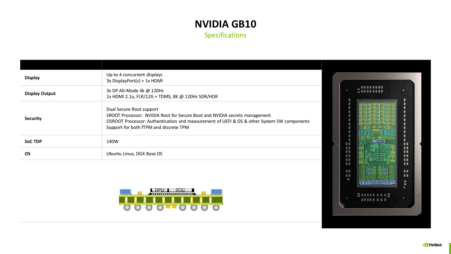
The GPU die supports up to 4 displays; 3 DisplayPort outputs and an HDMI 2.1a output.
The GB10 SoC’s is rated for a 140 Watt TDP.
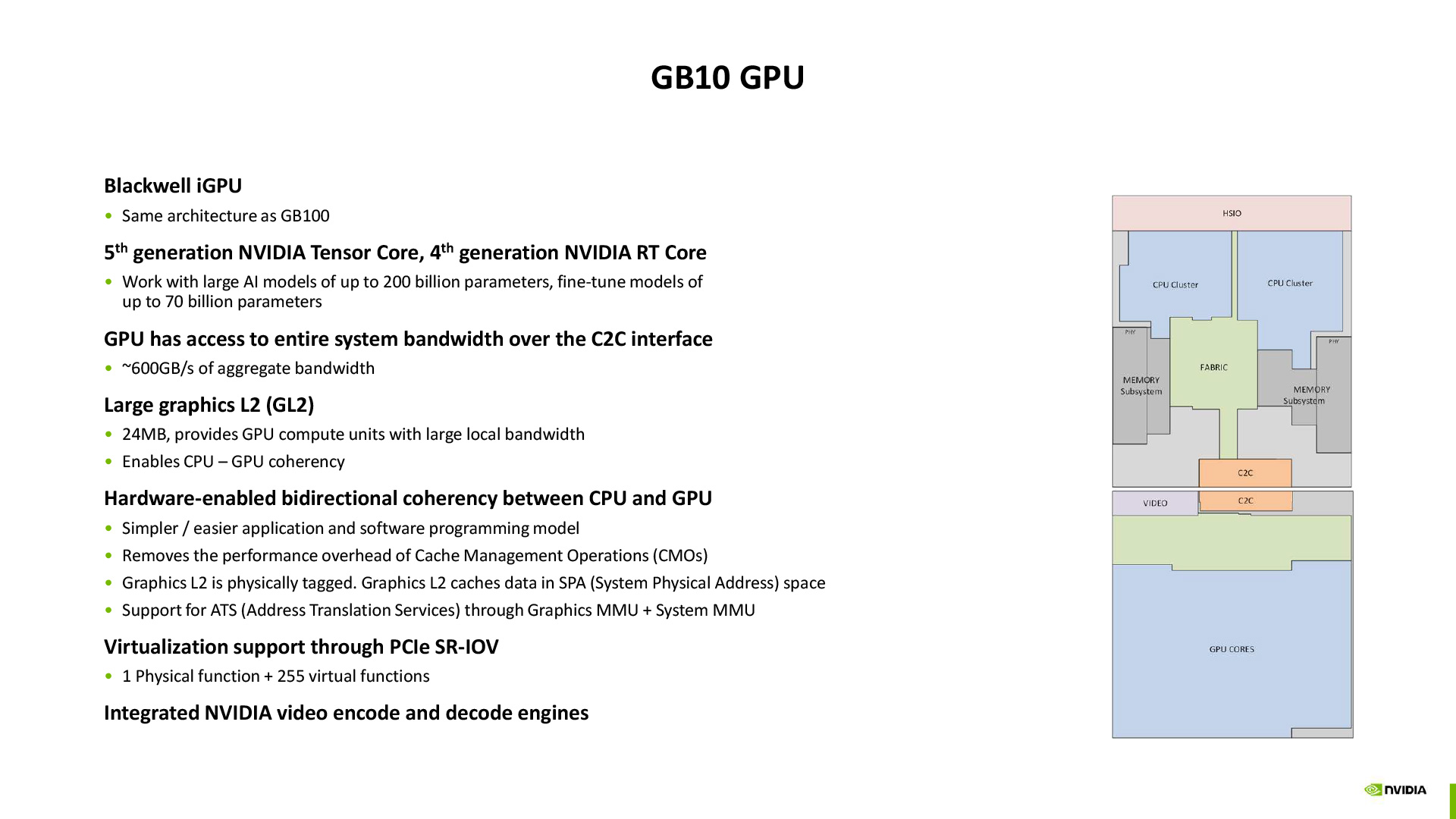
There’s a relatively large L2 cache of 24MB within the GPU die. This L2 is also what enables CPU/GPU coherency. That coherency, in turn, is managed at the hardware level. This removes some of the performance overhead, and simplifies things for developers.
Address translation services (ATS) are also implemented. This allows for the entire graphics L2 to be physically tagged.
The OS sees the GPU as a PCIe device. SR-IOV is supported.
And both an NVDEC and NVENC engine are present.
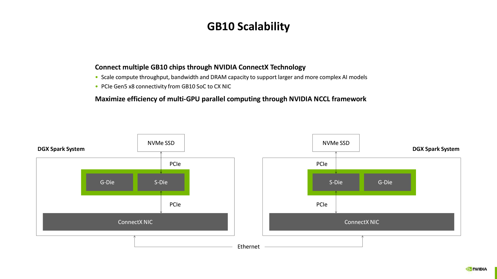
Each DGX Spark box includes a ConnectX-7 NIC, allowing two systems to be paired up, and the GB10 chips connected. PCIe 5.0 x8 backhaul from the SoC to the NIC. (Patrick notes that this means you only get 200Gbps to the NIC. So both ports can’t run at 200G at the same time)
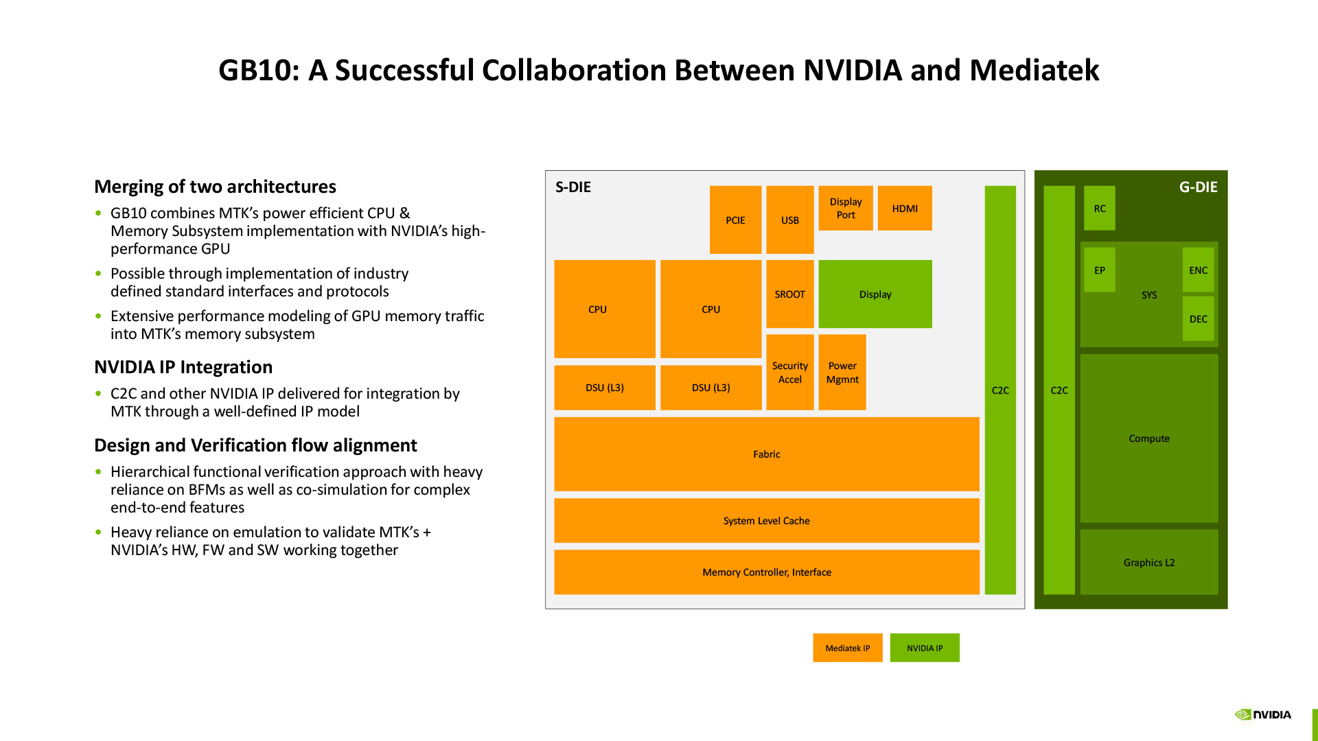
As noted earlier, this is a NVIDIA + MediaTek project, with the latter providing the CPU chiplet (S-die). This is a big deal, especially as the memory controller for the chip is on the CPU chiplet – so NVIDIA was reliant on MediaTek to deliver a performant and reliable memory subsystem.
This also meant that MediaTek implemented pieces of NVIDIA IP, including a display controller and C2C link.
And there was a whole lot of verification involved ahead of time in making sure this would all work. This seems to have paid off very well for NVIDIA, as GB10 worked on its very first spin, A0. No respins were needed to fix any design flaws.